
Overcoming Common Challenges in High-Density PCB Assembly
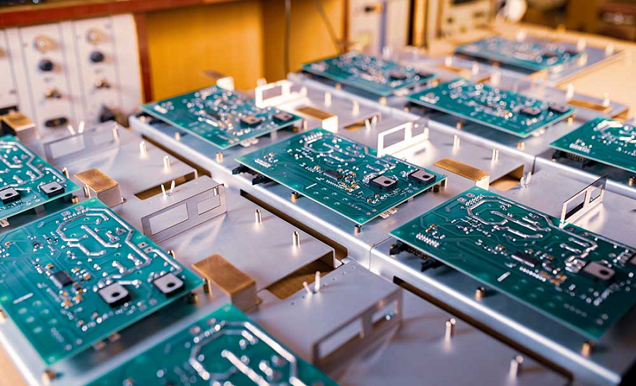
Image Source: www.topfastpcba.com
High-density printed circuit board (PCB) assembly is becoming increasingly common as electronic devices continue to shrink in size while growing in complexity. High-density PCB assemblies pack more components into a smaller area, which can lead to significant challenges during the manufacturing process. These challenges include managing signal integrity, heat dissipation, and the physical constraints of placing components on densely packed boards. However, with the right strategies and technologies, these challenges can be effectively managed to produce reliable, high-performance PCB assemblies.
Managing Signal Integrity
One of the primary challenges in high-density PCB assembly is maintaining signal integrity. As more components are packed into a smaller area, the risk of crosstalk and electromagnetic interference (EMI) increases. Crosstalk occurs when signals from one trace interfere with those of another, potentially causing data errors or signal degradation. EMI, on the other hand, can affect the performance of the entire PCB if not properly managed.
To overcome these issues, careful design practices must be implemented. This includes optimizing trace routing to minimize the length of high-speed signals, increasing the distance between parallel traces, and using shielding where necessary. Additionally, selecting materials with the appropriate dielectric constant and loss tangent can help reduce signal degradation. Working closely with a pcb assembly contract manufacturer that has experience with high-density designs is crucial, as they can provide valuable insights and recommendations during the design phase to ensure signal integrity is maintained.
Heat Dissipation
Heat dissipation is another critical challenge in high-density PCB assembly. As more components are placed on a board, the amount of heat generated increases, which can lead to overheating and potentially damage the components. Efficient thermal management is essential to prevent this and ensure the long-term reliability of the PCB.
Several strategies can be employed to manage heat in high-density PCB assemblies. One approach is to use thermal vias, which are small holes filled with conductive material that help transfer heat from the surface of the board to the internal layers or to an external heat sink. Another method is to incorporate heat spreaders or heat sinks directly onto the PCB to dissipate heat more effectively. Additionally, selecting components with lower power consumption and arranging them strategically to minimize heat accumulation can also help manage thermal challenges.
Thermal simulation tools can be used during the design phase to model the heat distribution across the PCB and identify potential hotspots. This allows for proactive adjustments to the design to improve thermal performance before the board goes into production.
Component Placement and Routing
The physical constraints of high-density PCB assembly present significant challenges when it comes to component placement and routing. With limited space, designers must carefully plan the layout to avoid conflicts between components and ensure that all connections can be made without crossing signals unnecessarily.
Advanced design techniques such as multi-layer PCB designs are often used to address these challenges. By adding more layers to the PCB, designers can route signals on different layers, effectively increasing the available routing area and reducing congestion on any single layer. This approach also allows for better separation of power and signal traces, which can improve overall performance.
Component placement must be done with consideration of not only space but also the functionality and reliability of the PCB. For example, sensitive components should be placed away from sources of EMI, and high-power components should be positioned in a way that allows for efficient heat dissipation.
Testing and Quality Assurance
Given the complexity of high-density PCB assemblies, thorough testing and quality assurance are critical to identify and address any potential issues before the final product is delivered. This includes functional testing, in-circuit testing (ICT), and automated optical inspection (AOI) to ensure that all components are correctly placed and functioning as intended.
Collaboration with a pcb assembly company experienced in high-density designs can also be beneficial during the testing phase. Such manufacturers often have advanced testing equipment and protocols in place to detect and resolve issues that may not be apparent during the design phase. This collaboration can significantly reduce the likelihood of defects in the final product, ensuring that the PCB performs reliably in its intended application.
Final Considerations
High-density PCB assembly presents a unique set of challenges, but with the right strategies and collaboration with experienced partners, these challenges can be successfully overcome. By focusing on signal integrity, heat dissipation, and careful component placement, manufacturers can produce high-density PCBs that meet the demands of today’s advanced electronic devices.